Technology area
Design guideTECHNOLOGY DRIVEN ELECTRONIC COMPANY
- Specifications of Manufacturing Process
Drill & Plating
Pattern & Coverlay
PSR & Marking Printing
Surface treatment & BBT
External Processing
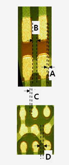
PSR
| Category | Item | Specifications | Other |
|---|---|---|---|
| PSR (ordinary) | S/M open | A=Land(Pad) +0.1mm |  |
| Interval between S/M open parts | B=Min 0.1mm (Solder Dam) | ||
| PSR paint thickness | 10±5㎛ | ||
| PSR application scope | All parts except the separation | ||
| Tilt allowance | ±5㎛ | ||
| PSR(BGA) | S/M open | C= BGA Land +0.07mm | |
| Tilt allowance | ±35㎛ | ||
| Paint interval / thickness | D=0.1mm / 20±5㎛ |
- S/M(solder mask) printing is performed on copper foil, using UV ink.
- Colors : green, yellow, and black.
Marking Plating
| Category | Item | Specifications | Other |
|---|---|---|---|
| Marking | A=line width | Min 0.13mm | |
| B=interval to land | Min 0.2mm | On edge | |
| Interval to out | Min 0.3mm | On edge | |
| Interval to separation | Min 0.5mm | On edge | |
| Interval to C/L open on GND copper plate | Min 0.2mm | On edge | |
| Tile allowance | ±0.15mm |


